(for basic information on Shift Register, head over to Technopedia section)
Things needed:-
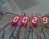
1) Arduino(any model will do)
2) 16 x LEDs
3) 2 x 74HC595N Shift register
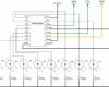
Pin arrangement of the shift register is given in the following diagram:-
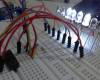
Connections:
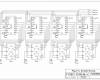
Connect the circuit as per the schematic given below

Code:-
For Binary Counting:
int dataPin = 2; //Define which pins will be used for the Shift Register control
int latchPin = 3;
int clockPin = 4;
int byte1 = 0; //The counter for storing the byte #1 value
int byte2 = 0; //The counter for storing the byte #2 value
void setup()
{
pinMode(dataPin, OUTPUT); //Configure each IO Pin
pinMode(latchPin, OUTPUT);
pinMode(clockPin, OUTPUT);
}
void loop()
{
for (byte2 = 0; byte2 < 256; byte2++) //Outer Loop
{
for (byte1 = 0; byte1 < 256; byte1++) //Inner Loop
{
digitalWrite(latchPin, LOW); //Pull latch LOW to start sending data
shiftOut(dataPin, clockPin, MSBFIRST, byte1); //Send the data byte 1
shiftOut(dataPin, clockPin, MSBFIRST, byte2); //Send the data byte 2
digitalWrite(latchPin, HIGH); //Pull latch HIGH to stop sending data
delay(250);
}
}
}
For LED rider:
int dataPin = 2; //Define which pins will be used for the Shift Register control
int latchPin = 3;
int clockPin = 4;
int seq1[14] = {1,2,4,8,16,32,64,128,64,32,16,8,4,2}; //The array for storing the
// byte #1 value
int seq2[14] = {128,64,32,16,8,4,2,1,2,4,8,16,32,64}; //The array for storing the
// byte #2 value
void setup()
{
pinMode(dataPin, OUTPUT); //Configure each IO Pin
pinMode(latchPin, OUTPUT);
pinMode(clockPin, OUTPUT);
}
void loop()
{
for (int x = 0; x < 14; x++) //Array Index
{
digitalWrite(latchPin, LOW); //Pull latch LOW to start sending data
shiftOut(dataPin, clockPin, MSBFIRST, seq1[x]); //Send the data byte 1
shiftOut(dataPin, clockPin, MSBFIRST, seq2[x]); //Send the data byte 2
digitalWrite(latchPin, HIGH); //Pull latch HIGH to stop sending data
delay(75);
}
}
YOU MAY EXPERIMENT WITH 4 SHIFT REGISTERS too and so on...